


Researchers from China and the U.S. have jointly created a new type of stable semiconductor graphene, which displays performance 10 times higher than silicon and 20 times larger than that of the other two-dimensional semiconductors. The achievement marks "a leap from silicon chips to carbon chips," Ma Lei, leader of the research from the Tianjin International Center for Nanoparticles and Nanosystems (TICNN) at Tianjin University, who led the research, told the Global Times.
The achievement, jointly made by Ma's team and researchers from School of Physics, Georgia Institute of Technology in the U.S., was published online on the website of the journal "Nature" on January 3, 2024.
With silicon-based chips gradually approaching the physical limit of two nanometers, there is a surge in global demand for chips based on high-quality semiconductor materials. Two-dimensional materials, due to their excellent electronic transport properties and potential for high integration, have become a new frontier that scientists and semiconductor companies around the world are eager to invest in.
Graphene, as the first discovered two-dimensional material that can exist stably at room temperature, has been the focus of scientists' efforts since its discovery in 2004 to design a new type of chip that consumes less energy and operates faster than existing semiconductors. However, the unique Dirac Cones of graphene leads to its "zero bandgap" characteristic, which has been the biggest obstacle to its application in the semiconductor field.
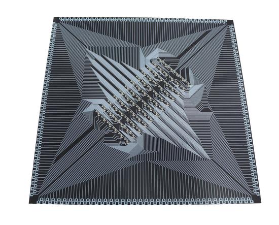
By precisely controlling the epitaxial growth process of graphene, Ma's team introduced a bandgap into graphene, creating a new type of stable semiconductor graphene, which exhibits electron mobility far exceeding that of silicon materials. It displays performance 10 times higher than silicon and 20 times larger than that of the other two-dimensional semiconductors.
"We mainly applied a special growth environment and growth conditions to modulate graphene itself using SiC crystals, achieving the opening of a bandgap in graphene. This transforms the originally gapless graphene into a material with a bandgap," Ma said. He noted that what the team created “is a true single-crystal graphene semiconductor.”
The development of this semiconductor not only paves the way for high-performance electronic devices surpassing traditional silicon-based technologies but also injects new impetus into the entire semiconductor industry. As the limits predicted by Moore's Law draw closer, the emergence of semiconductor graphene heralds a fundamental shift in the field of electronics. Its breakthrough properties meet the growing demand for higher computing speeds and miniaturized integrated electronic devices, read a report on the Tianjin University's website.
Once delivered into large scale production, the single-crystal semiconductor graphene will lay an important foundation for the transition from the silicon era to the carbon era. However, whether graphene semiconductors can lead to a breakthrough in the chip industry still needs time to test, Ma noted.
When asked how far the achievement is from industrialization, Ma said he currently cannot predict. "When it can be put into large-scale industrial applications depends on the process from millimeter-scale single crystals to inch-scale single crystals."
In a related report on January 4 by yicai.com, Ma was quoted as saying that “I estimate that it will take another 10 to 15 years before graphene semiconductors can truly be fully implemented.”
Ma said that now he and his team are working hard to grow larger-sized graphene semiconductor single crystals.
In order to continue to promote the development of semiconductors, countries and regions all over the world are actively seeking new materials and paradigms in addition to two-dimensional materials. In November 2023, Huawei and Harbin Institute of Technology jointly applied for a "hybrid bonding method for three-dimensional integrated chips based on silicon and diamond." In September 2023, Japanese news outlet Nikkei reported that the Japanese startup company OOKUMA plans to commercialize diamond semiconductors, and will start production as early as the fiscal year 2026.
With the intensification of competition, the U.S. has been increasing its export control measures on chips to China, unreasonably suppressing Chinese semiconductor companies, and attempting to "strangle" China in the semiconductor chip field.
In this context, the achievement by Chinese and American teams has attracted special attention. According to Ma, the intensification of China-U.S. semiconductor competition has indeed had an impact on the cooperation between the scientific teams of the two countries, such as information exchange and sample exchange. However, overall, the cooperation between the two teams has been fruitful.
"Healthy competition is an important factor in promoting development, while malicious competition hinders the development of technology. I hope that cooperation is the mainstream and competition is a stimulant. With cooperation as the mainstream, appropriate competition will make scientific development better and better," Ma noted.


 京公網安備 11010202009201號